- 您现在的位置:买卖IC网 > Sheet目录3880 > PIC24F08KL302-I/SO (Microchip Technology)IC MCU 16BIT 8KB FLASH 28-SOIC
2011 Microchip Technology Inc.
DS31037B-page 34
PIC24F16KL402 FAMILY
4.2.2
DATA MEMORY ORGANIZATION
AND ALIGNMENT
To maintain backward compatibility with PIC devices
and improve data space memory usage efficiency, the
PIC24F instruction set supports both word and byte
operations. As a consequence of byte accessibility, all
Effective Address (EA) calculations are internally
scaled to step through word-aligned memory. For
example, the core recognizes that Post-Modified
Register Indirect Addressing mode [Ws++] will result in
a value of Ws + 1 for byte operations and Ws + 2 for
word operations.
Data byte reads will read the complete word, which
contains the byte, using the LSB of any EA to
determine which byte to select. The selected byte is
placed onto the LSB of the data path. That is, data
memory and the registers are organized as two
parallel, byte-wide entities with shared (word) address
decode, but separate write lines. Data byte writes only
write to the corresponding side of the array or register,
which matches the byte address.
All word accesses must be aligned to an even address.
Mis-aligned word data fetches are not supported, so
care must be taken when mixing byte and word
operations, or translating from 8-bit MCU code. If a
mis-aligned read or write is attempted, an address error
trap will be generated. If the error occurred on a read,
the instruction underway is completed; if it occurred on
a write, the instruction will be executed, but the write
will not occur. In either case, a trap is then executed,
allowing the system and/or user to examine the
machine state prior to execution of the address Fault.
All byte loads into any W register are loaded into the
LSB; the MSB is not modified.
A Sign-Extend (SE) instruction is provided to allow the
users to translate 8-bit signed data to 16-bit signed
values. Alternatively, for 16-bit unsigned data, users
can clear the MSB of any W register by executing a
Zero-Extend (ZE) instruction on the appropriate
address.
Although most instructions are capable of operating on
word or byte data sizes, it should be noted that some
instructions operate only on words.
4.2.3
NEAR DATA SPACE
The 8-Kbyte area between 0000h and 1FFFh is
referred to as the Near Data Space (NDS). Locations in
this space are directly addressable via a 13-bit abso-
lute address field within all memory direct instructions.
The remainder of the data space is addressable
indirectly. Additionally, the whole data space is
addressable using MOV instructions, which support
Memory Direct Addressing (MDA) with a 16-bit address
field. For PIC24F16KL402 family devices, the entire
implemented data memory lies in Near Data Space.
4.2.4
SFR SPACE
The first 2 Kbytes of the Near Data Space, from 0000h
to 07FFh, are primarily occupied with Special Function
Registers (SFRs). These are used by the PIC24F core
and peripheral modules for controlling the operation of
the device.
SFRs are distributed among the modules that they
control and are generally grouped together by the
module. Much of the SFR space contains unused
addresses; these are read as ‘0’. The SFR space,
where the SFRs are actually implemented, is provided
in Table 4-2. Each implemented area indicates a
32-byte region, where at least one address is
implemented as an SFR. A complete listing of
implemented SFRs, including their addresses, is
provided in Table 4-3 through Table 4-18.
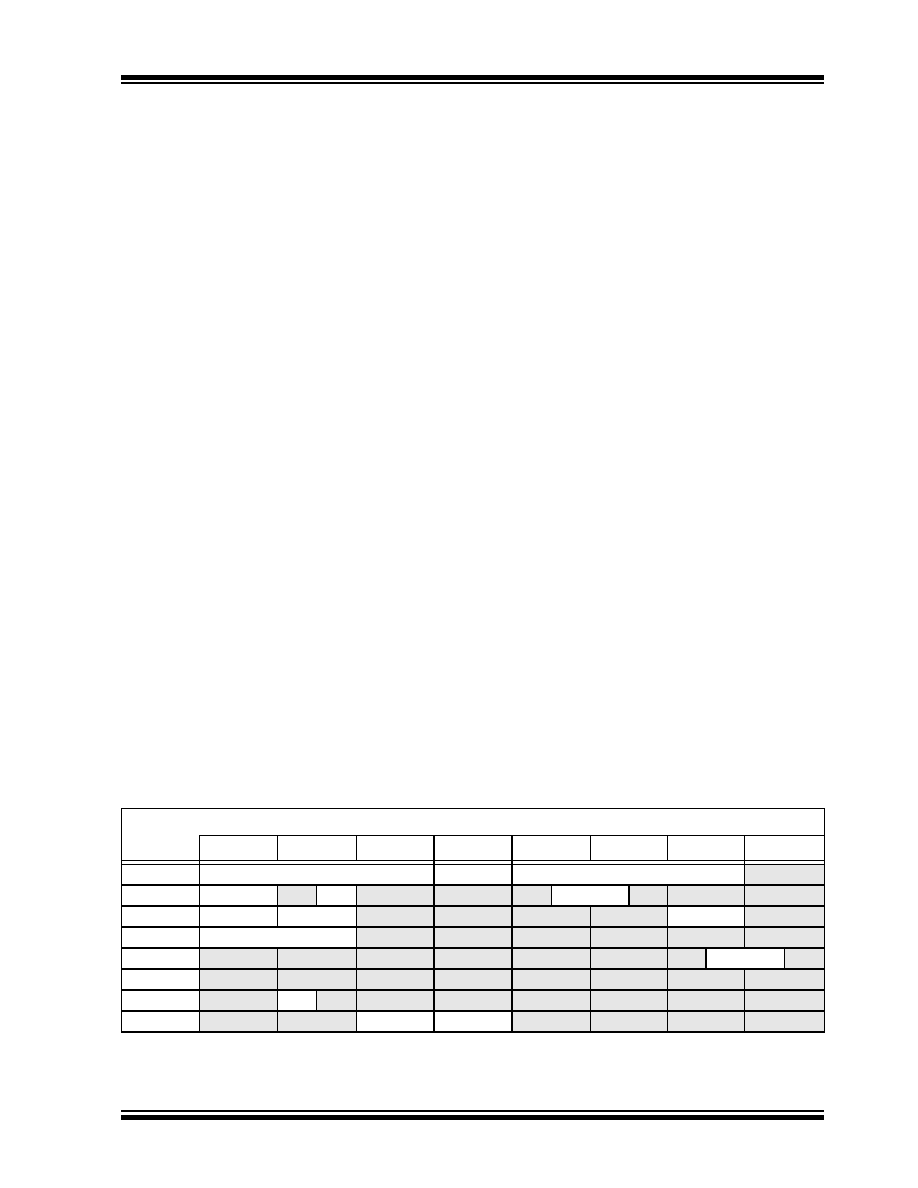
TABLE 4-2:
IMPLEMENTED REGIONS OF SFR DATA SPACE
SFR Space Address
xx00
xx20
xx40
xx60
xx80
xxA0
xxC0
xxE0
000h
Core
ICN
Interrupts
—
100h
Timers
—TMR
—
CCP
—
200h
MSSP
UART
—
I/O
—
300h
A/D
—
400h
—
ANSEL
—
500h
—
600h
—CMP
—
700h
—
System
NVM/PMD
—
Legend:
— = No implemented SFRs in this block.
发布紧急采购,3分钟左右您将得到回复。
相关PDF资料
XF2L-0535-1
CONN FPC 5POS 0.5MM SMT
PIC18LF23K22-I/SS
IC PIC MCU 8KB FLASH 28SSOP
PIC16LF1933-I/ML
IC PIC MCU FLASH 4K 28-QFN
PIC16F1933-I/ML
IC MCU 8BIT FLASH 28-QFN
PIC16F785-I/ML
IC PIC MCU FLASH 2KX14 20QFN
XF2L-0425-1
CONN FPC 4POS 0.5MM SMT
PIC16F1933-I/MV
IC MCU 8BIT FLASH 28-UQFN
PIC16F785-I/SO
IC PIC MCU FLASH 2KX14 20SOIC
相关代理商/技术参数
PIC24F08KL302-I/SP
功能描述:16位微控制器 - MCU 8KB FLASH 1KB RAM 256B 3V RoHS:否 制造商:Texas Instruments 核心:RISC 处理器系列:MSP430FR572x 数据总线宽度:16 bit 最大时钟频率:24 MHz 程序存储器大小:8 KB 数据 RAM 大小:1 KB 片上 ADC:Yes 工作电源电压:2 V to 3.6 V 工作温度范围:- 40 C to + 85 C 封装 / 箱体:VQFN-40 安装风格:SMD/SMT
PIC24F08KL302-I/SS
功能描述:16位微控制器 - MCU 8KB FLASH 1KB RAM 512B 3V 10-BIT ADC RoHS:否 制造商:Texas Instruments 核心:RISC 处理器系列:MSP430FR572x 数据总线宽度:16 bit 最大时钟频率:24 MHz 程序存储器大小:8 KB 数据 RAM 大小:1 KB 片上 ADC:Yes 工作电源电压:2 V to 3.6 V 工作温度范围:- 40 C to + 85 C 封装 / 箱体:VQFN-40 安装风格:SMD/SMT
PIC24F08KL302T-I/ML
功能描述:16位微控制器 - MCU 8KB FLASH 1KB RAM 512B 3V 10-BIT ADC RoHS:否 制造商:Texas Instruments 核心:RISC 处理器系列:MSP430FR572x 数据总线宽度:16 bit 最大时钟频率:24 MHz 程序存储器大小:8 KB 数据 RAM 大小:1 KB 片上 ADC:Yes 工作电源电压:2 V to 3.6 V 工作温度范围:- 40 C to + 85 C 封装 / 箱体:VQFN-40 安装风格:SMD/SMT
PIC24F08KL302T-I/MQ
功能描述:16位微控制器 - MCU 8KB FL 1KB RAM 256B 3V RoHS:否 制造商:Texas Instruments 核心:RISC 处理器系列:MSP430FR572x 数据总线宽度:16 bit 最大时钟频率:24 MHz 程序存储器大小:8 KB 数据 RAM 大小:1 KB 片上 ADC:Yes 工作电源电压:2 V to 3.6 V 工作温度范围:- 40 C to + 85 C 封装 / 箱体:VQFN-40 安装风格:SMD/SMT
PIC24F08KL302T-I/SO
功能描述:16位微控制器 - MCU 8KB FLASH 1KB RAM 512B 3V 10-BIT ADC RoHS:否 制造商:Texas Instruments 核心:RISC 处理器系列:MSP430FR572x 数据总线宽度:16 bit 最大时钟频率:24 MHz 程序存储器大小:8 KB 数据 RAM 大小:1 KB 片上 ADC:Yes 工作电源电压:2 V to 3.6 V 工作温度范围:- 40 C to + 85 C 封装 / 箱体:VQFN-40 安装风格:SMD/SMT
PIC24F08KL302T-I/SS
功能描述:16位微控制器 - MCU 8KB FLASH 1KB RAM 512B 3V 10-BIT ADC RoHS:否 制造商:Texas Instruments 核心:RISC 处理器系列:MSP430FR572x 数据总线宽度:16 bit 最大时钟频率:24 MHz 程序存储器大小:8 KB 数据 RAM 大小:1 KB 片上 ADC:Yes 工作电源电压:2 V to 3.6 V 工作温度范围:- 40 C to + 85 C 封装 / 箱体:VQFN-40 安装风格:SMD/SMT
PIC24F08KL401
制造商:MICROCHIP 制造商全称:Microchip Technology 功能描述:Low-Power, Low-Cost, General Purpose 16-Bit Flash Microcontrollers with nanoWatt XLP Technology
PIC24F08KL401-I/MQ
功能描述:16位微控制器 - MCU 8KB FLASH 1KB RAM 512B 3V 10-BIT ADC RoHS:否 制造商:Texas Instruments 核心:RISC 处理器系列:MSP430FR572x 数据总线宽度:16 bit 最大时钟频率:24 MHz 程序存储器大小:8 KB 数据 RAM 大小:1 KB 片上 ADC:Yes 工作电源电压:2 V to 3.6 V 工作温度范围:- 40 C to + 85 C 封装 / 箱体:VQFN-40 安装风格:SMD/SMT